Its special properties high transmission above 90 low resistivity n-type degenerate semiconductor behavior and wide direct band gap of 36 eV make it suitable for a number of applications such as electrochromic devices liquid crystal displays plasma displays. The lattice parameter is an important piece of information that can be derived from the X-ray diffraction data.
Materials Free Full Text Investigating The Defect Structures In Transparent Conducting Oxides Using X Ray And Neutron Scattering Techniques Html
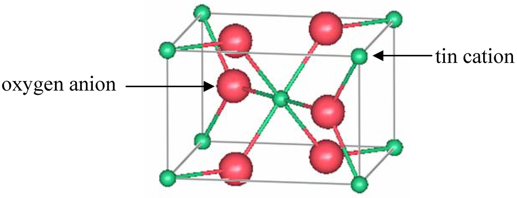
Indium tin oxide is typically encountered as an oxygen-saturated composition with a formulation of 74 In 18 O2 and 8 Sn by weight.
Indium tin oxide lattice parameter. Increasing deposition rate and film thickness changed the. The lattice parameter of these films was determined to be 0948 and 1026 nm for CTO and ITO respectively. Eight Sn-doped In2O3 ITO target materials for direct-current DC magnetron sputtering showing various rates of nodule formation were subjected to analyses of lattice parameter relative.
The posterior reduction of these parameters for a SnIn ratio above 5 can be explained as due to the limit of solubility of tin in indium oxide and a possible formation of neutral complexes of tin inside the indium oxide lattice. Lattice parameters of ITO are a 104 Å and FTO are a 48Åandc 34 Å respectively. Indium oxide is used in some types of batteries thin film infrared reflectors transparent for visible light hot mirrors some optical coatings and some antistatic coatings.
It is known that the indium oxide lattice parameter expands beyond the undoped value of 10118 Å as tin is incorporated. Much of the SnIV likely exists as interstitial atoms in the indium oxide cubic bixbyite lattice rather than as replacement atoms. Additionally the Taguchi method of experimental design was.
So In2O3 is doped with Sn as ionic radii of Sn is less than In. Structural electrical and optical properties of the films were then examined. The crys-tal structures and respective lattice parameters are found to be consistent with the literature 12 15 36 37.
No other tin phases could be identified from the cubic indium tin oxide. When the wt of the Indium is less 2080 than Sn some of the tin oxide peaks observed and indicated in star symbol. This leads to the formation of one of the best transparent conductive oxides TCOs namely indium-tin oxide ITO.
By doping the host lattice with another lattice having less ionic radii than the host. The size parameters measured over five frames of 50mm 50mm scanning electron microscopy SEM. Doping with tin increases the oxygencation ratio and the lattice parameter.
Indium tin oxide ITO thin films on polycarbonate PC substrates were patterned using the laser direct-write LDW technique to form an isolation line. These thin films possess low resistivities in the 10 -4 Ω cm range Hall mobilities up to 30 cm 2 V s and carrier concentrations in the 10 20 cm -3 range. Hence Indium tin oxide ITO has been widely studied by many prestigious research groups.
The 222 and 400 plane is ascribed for oxygen efficient and deficient nature of ITO films 41. Although the radii of Sn 4 071 Å are smaller than the In 3 081 Å for which it substitutes the net positive charge results in an electrostatic repulsive force that expands the doped lattice 24. Here tin acts as a cationic dopant in the In 2 O 3 lattice and as a substitute on the indium sites to bind with the interstitial oxygen.
The effect of the LDW parameters power pulse repetition rate and defocusing distance on the isolation line width depth and roughness of the PC within the line was investigated. Other samples were reduced in forming gas and magnetic low-temperature susceptibility measure-ments with a superconducting quantum interference device SQUID were used as the detection method for traces of metallic indium and tin. Both samples are highly crystalline in nature as evidenced by the sharp easily discernable peaks in their diffractograms.
Oxygen admixture and sputtering deposition parameters were optimized to obtain the highest transparency as well as lowest resistivity. Depending on the oxygen content it can either be described as a ceramic or alloy. Indium tin oxide is a ternary composition of indium tin and oxygen in varying proportions.
The stoichiometry In sub 32-xSn sub xO sub 48x2. Indium tin oxide ITO is a well known n-type transparent conducting oxide material. In order to confirm the nanocrys-.
Structural changes in the indium oxide lattice due to doping with Sn4ITO were studied by Mossbauer spectroscopy EXAFS and neutron powder diffraction. In combination with tin dioxide indium oxide forms indium tin oxide also called tin doped indium oxide or ITO a material used for transparent conductive coatings. Crystal grain size depends on processing parameters eg deposition rate and substrate temperature.
Both parameters present their maximum for SnIn 5. Indiumtin-oxide nanoparticles by solid-state reaction 19 where k is a particle-geometry-dependent constant for spherical shape k 1 λ is the wavelength used λ 15406Åβ isthefull-widthathalf-maximumFWHMand θ is the diffracted angle. This method makes use of the su-perconductivity of the metals below 34 K.
There is a decrease in electrical conductivity as the tin content and oxygen partial pressure increase which is related to a distortion in the first SnO shell. Mulitiple of the lattice constant. Normally the 30 of Sn is needed to exhibiting the SnO 2 diffraction lines in ITO.
X0-6 is taken to understand the change in lattice parameter electronic structure and optical property of ITO. Indium tin oxide ITO is the most well-known and utilized transparent conductive oxide TCO but also the most expensive. The Indium wt is equal with Sn 5050 or more 8020 is clearly observed from the XRD pattern.
The estimated average crystallite size is found to be 47nm. Properties of silver indium tin oxide ITO and indium zinc oxide IZO. Oxygen-saturated compositions are so typical that unsaturated compositions are termed.
Following the approach shown in Fig. 1 we first fabricated the PAN nanostructures. Tin substitutes for indium in ITO crystals forming either stannous oxide tinII monoxide or stannic oxide tinIV dioxide at the doping levels commonly used 8-10.
Eight Sn-doped In 2 O 3 ITO target materials for direct-current DC magnetron sputtering showing various rates of nodule formation were subjected to analyses of lattice parameter relative density electrical properties optical absorption spectra in 05-5 eV and oxygen deficiency δ in In 0905 Sn 0095 2 O 3x-δThe δ value was evaluated by heating the sample powders in a closed. Experimentally observed that 6 tin doping in indium oxide is suitable for optoelectronic applications and more doping beyond this limit degrades the optoelectronic property. Indium tin oxide ITO films were sputtered on corning glass substrate.
The lower values of a compared to the bulk value a_ mathrm bmathrm umathrm lmathrm k 10118 Å 13 may be attributed to the substitution of In by Sn which has a smaller ionic radius resulting in a smaller In 2 O 3 lattice 2 19 34 35. Indium tin oxide ITO thin films are being the most used material the interest of which has been trusted by fundamental advantages over the competing materials. The lattice parameter a are calculated in this case by means of the plane-spacing equation for cubic crystal which is give by.
Many aspects of ITO ceramics as an important raw materials of ITO films are studied as well in the last.

The Effect Of Post Annealing On Indium Tin Oxide Thin Films By Magnetron Sputtering Method Sciencedirect

Crystal Structure Of Sno P4 Nmm The Lattice Parameters Are Download Scientific Diagram


Tidak ada komentar